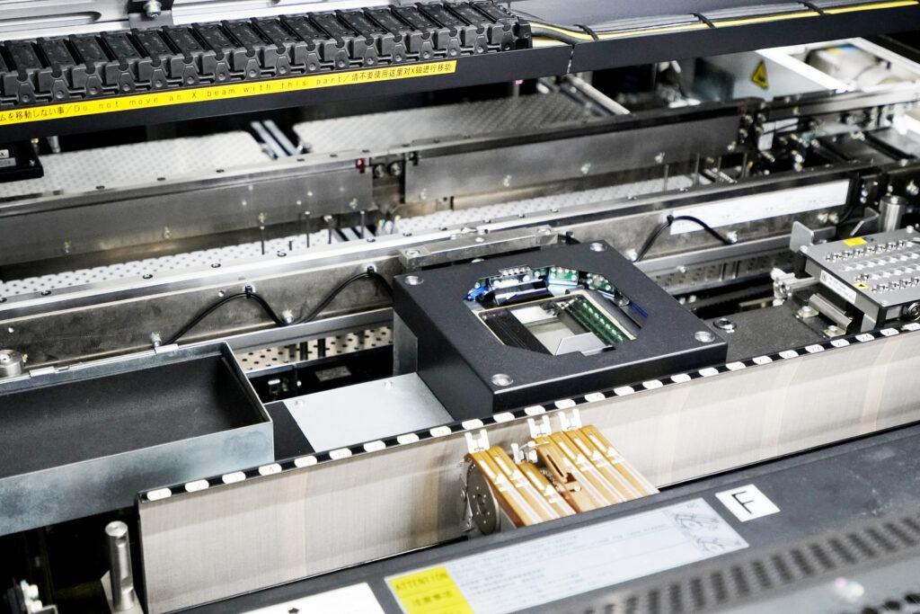
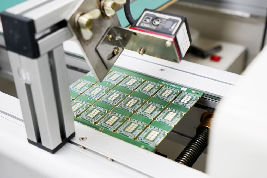
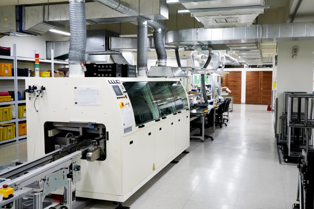
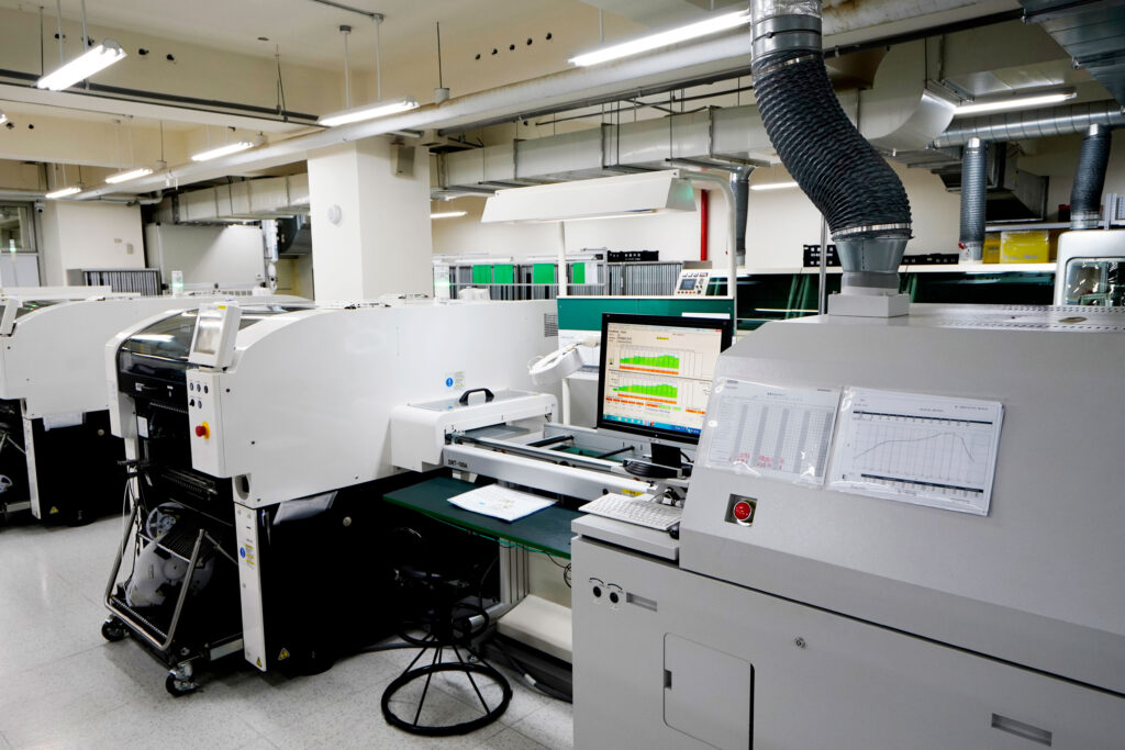
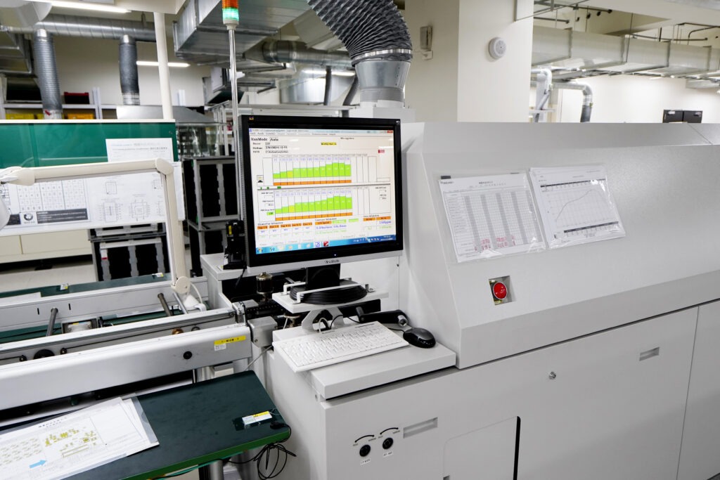
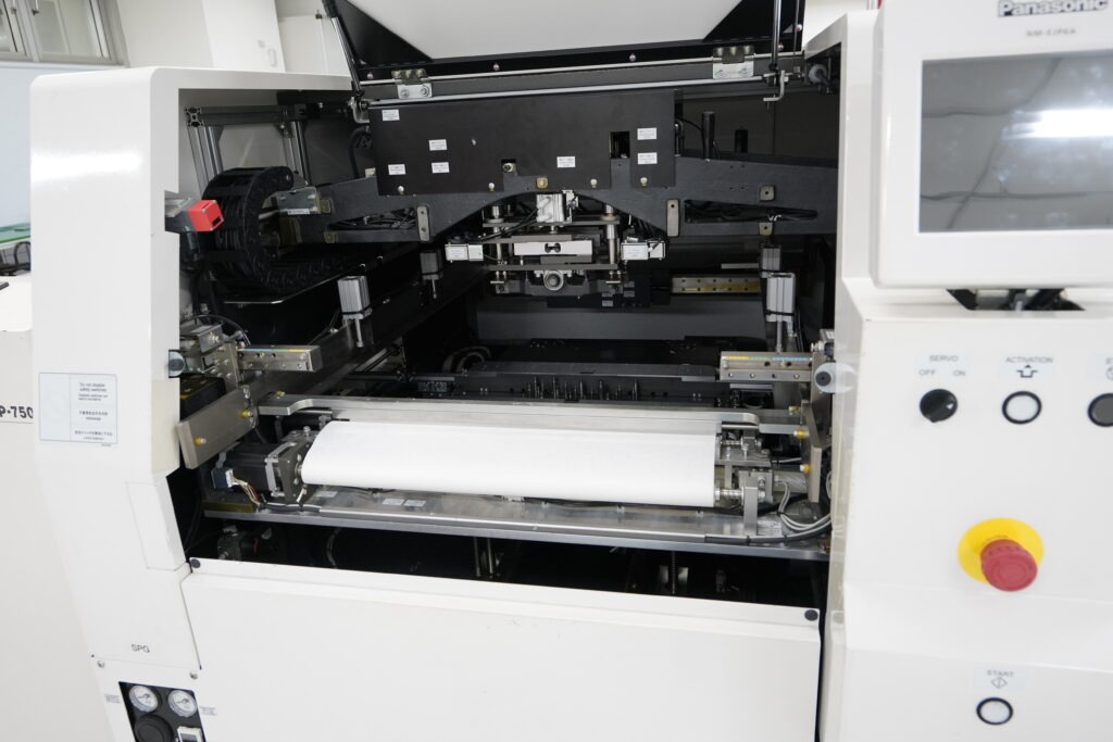
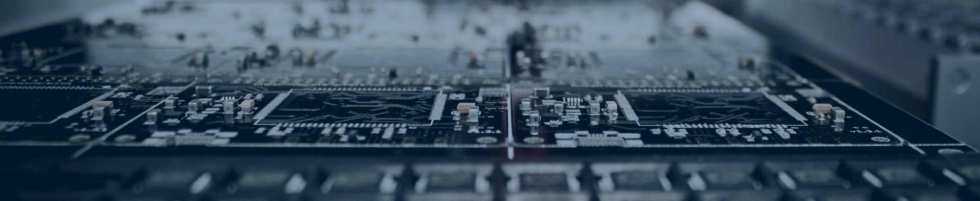
TechNexion maintains advanced manufacturing facilities designed to meet the highest standards of quality, reliability, and compliance. Our rigorous processes and certified management systems ensure we consistently deliver excellence.
Our commitment to quality and continuous improvement is demonstrated through the following internationally recognized certifications:
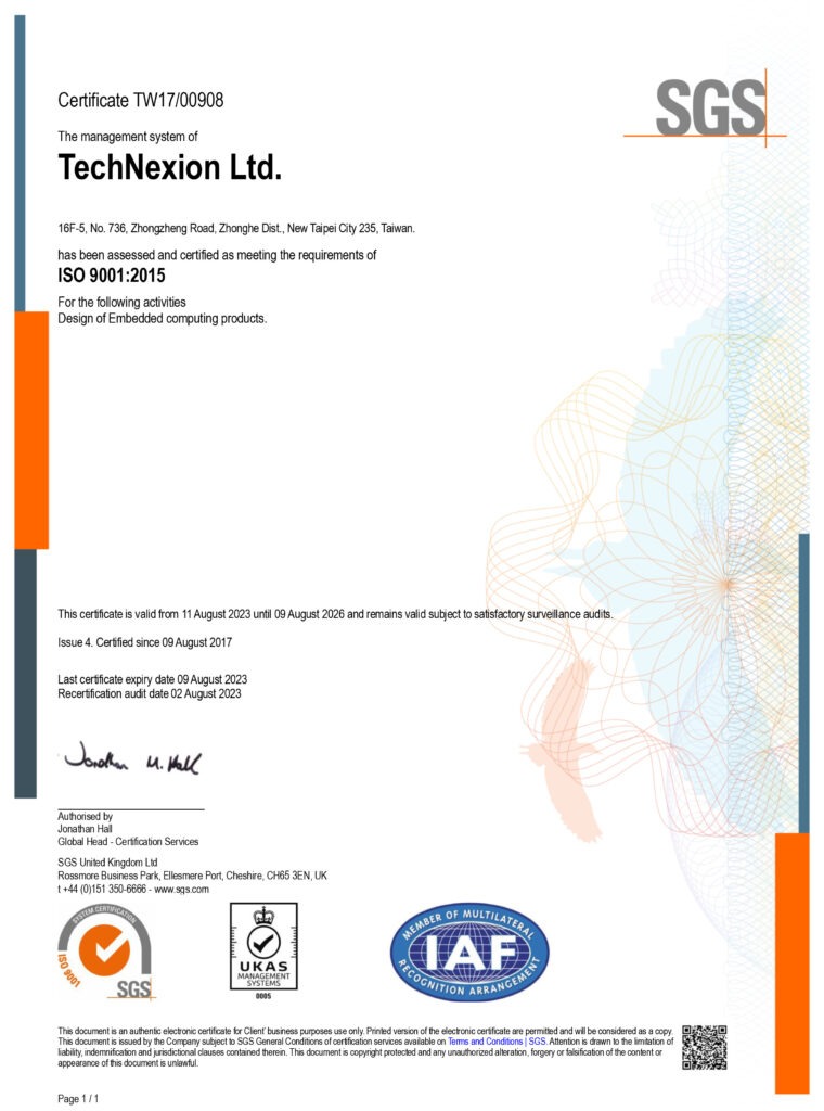
ISO 9001:2015
This certification ensures the consistent delivery of products and services that meet customer requirements and regulatory standards. It emphasizes strong customer focus, effective management involvement, systematic processes, and continuous improvement to maintain high quality and customer satisfaction.
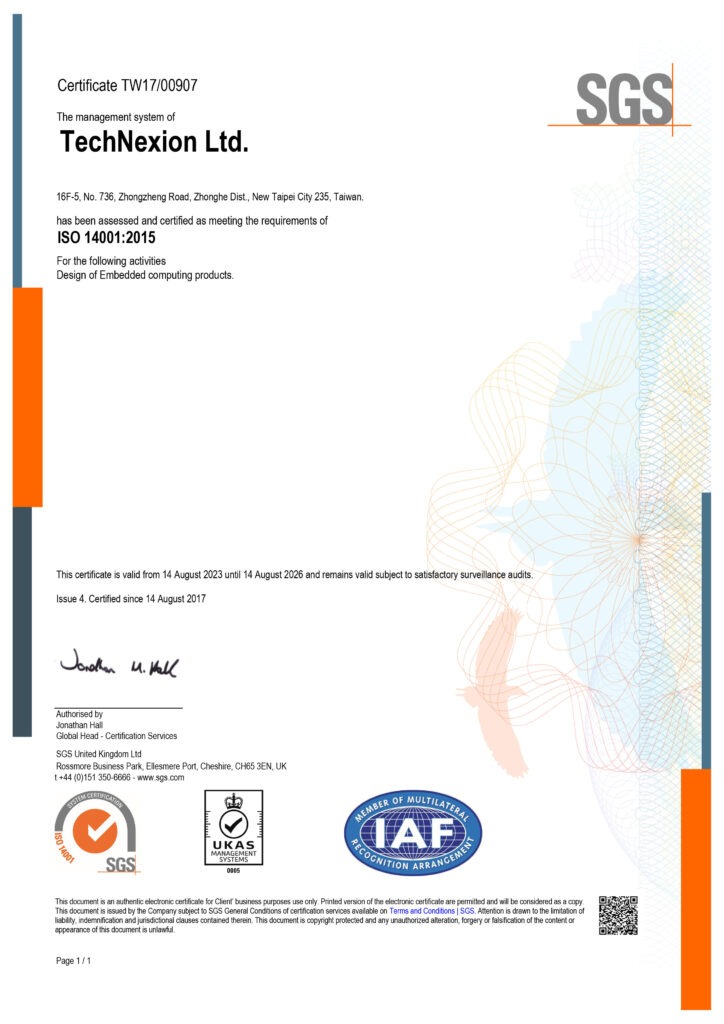
This standard enables us to systematically manage our environmental responsibilities, identifying and controlling environmental impact across our operations. It guides us in minimizing waste, conserving resources, and reducing our environmental footprint, thereby contributing effectively to global sustainability.
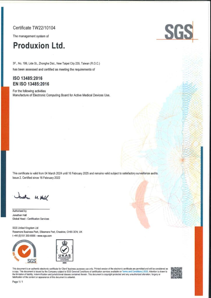
Specifically tailored for the medical device industry, ISO 13485 emphasizes strict compliance with regulatory requirements and quality standards. This certification highlights our capability to consistently produce reliable medical-grade products, ensuring safety, efficacy, and customer confidence in healthcare applications.